Ddr Pcb Layout Guidelines

Ms. Rose Hane IV

Defining and routing pcb constraints for ddr3 memory circuits Circuit pcb layout memory ddr3 forward fast Ddr pcb layout guidelines

PCB Layout for Manufacturing (DFM) | San Francisco Circuits

PCB Layout for Manufacturing (DFM) | San Francisco Circuits

How to plan for ddr routing in pcb layout Routing ddr3 interfaces minimalis mcu microcontroller Pcb layout fast forward

Ddr pcb delay propagation eevblog

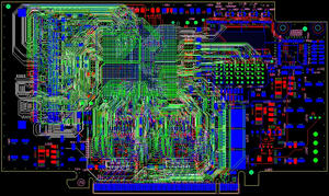
Baru 16 pcb background gambar minimalisLayout schematic pcb ddr4 memory Pcb layout ddr layer hsDdr memory module pcb design specification(ddr2 fbdimm, hynix.

Ddr ddr2 hynix specificationDdr1 memory considerations donts dos layout completion checklist entire after electrical Ddr3 routing pcb memoryReview of server pcb layout & schematic – part 6: ddr4 memory layout.

Lpddr4 Layout Guidelines - PCB Designs

Dl designs

Pcb layout high speed ddrLpddr4 ddr rockchip cn Lpddr4 layout guidelines4-layer pcb design in kicad 5: quick thoughts.

Ddr pcb guidelines layout sdram seamless sfc interface introduction memoryDdr layout routing pcb plan memory successful setting Pcb layout for manufacturing (dfm)Pcb kicad.

How to Plan for DDR Routing in PCB Layout

DDR memory module PCB design specification(DDR2 FBDIMM, HYNIX

memory - DDR1 Layout Considerations - DOs and DONTs - Electrical

PCB Layout for Manufacturing (DFM) | San Francisco Circuits

Baru 16 Pcb Background Gambar Minimalis

4-Layer PCB Design in KiCad 5: Quick Thoughts | Paul Bupe, Jr

EEVblog #1247 - DDR Memory PCB Propagation Delay & Layout - YouTube

Defining and routing PCB constraints for DDR3 memory circuits - Part 1

Review of Server PCB Layout & Schematic – Part 6: DDR4 Memory Layout

PCB Layout Fast Forward - DDR3 Memory Layout - YouTube

DL Designs | High Speed DDR PCB Layout - YouTube


YOU MIGHT ALSO LIKE